X

Partner Login

Enter your username and password here on order to log in on the partner portal:

No registered partner yet?

Register now

What Is an FPGA Chip Used For?

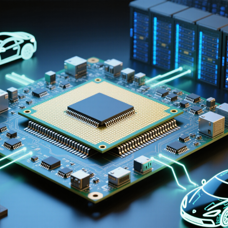
An Fpga Chip is not a fixed-function component. Engineers can configure its logic after manufacturing, then adapt it as a product’s needs change. That makes it useful in telecommunications equipment, industrial controls, automotive systems, and data-center acceleration. Picture a network device handling changing workloads without replacing its underlying hardware. The chip’s logic can be reconfigured. That flexibility has limits, though: design, verification, and power use still demand careful engineering.

The market reflects growing interest. Grand View Research estimated the global FPGA market at about $11.1 billion in 2023 and forecast an 8.4% compound annual growth rate from 2024 to 2030. This is a market estimate, not proof that every application benefits from programmable logic. For a small, stable task, a fixed-function chip may be cheaper or more efficient. The right choice depends on workload, latency, power, and product lifespan.

FPGA pioneer Ross Freeman’s term “field-programmable gate array” captures the core idea: hardware logic can be configured in the field. That remains a useful way to understand what these chips do. They can process data in parallel and respond predictably, which matters in systems that cannot tolerate unnecessary delay. Yet flexibility is not magic. A poorly designed FPGA implementation can waste resources or miss performance targets. This article explores what an Fpga Chip is used for, where it fits, and what engineers should weigh before choosing one.
What Is an FPGA Chip Used For?

What Is an FPGA Chip?

An FPGA, or field-programmable gate array, is a chip whose internal digital circuits can be configured after manufacturing. It contains logic blocks, programmable connections, and input/output circuits. Together, these resources can be arranged to perform specific tasks. A CPU generally follows instructions in sequence; an FPGA can process many operations in parallel. That matters. Engineers describe the design in a hardware language, then configure the chip with a bitstream. They can revise that configuration without changing the physical chip.

For example, an FPGA might process camera pixels while handling sensor signals, or control a motor with tightly timed inputs. Its design can be adjusted when requirements change. But flexibility is not free: development, testing, power use, and timing constraints still demand careful engineering.

The World Semiconductor Trade Statistics Spring 2025 forecast put worldwide semiconductor sales at $700.9 billion for 2025, an 11.2% increase over 2024. This figure describes the wider chip industry, not FPGA sales specifically.

It offers useful context: programmable logic is one option among many in a large and changing hardware landscape. The trade-off is easy to underestimate.

How Is an FPGA Chip Configured?

What Is an FPGA Chip Used For?

An FPGA chip is used when a digital circuit needs to be changed or tailored after the hardware is made. Its configurable logic blocks and routing connections can form functions such as signal filters, timing controllers, or data-processing pipelines. Engineers describe the desired behavior in a hardware description language. Design tools then synthesize the logic, fit it to the chip, and generate a configuration bitstream. That bitstream sets the chip’s logic and connections. Some devices retain configuration without power; others must load it again at startup.

Tips: Check the device’s configuration method before designing a startup process. Keep a known-good bitstream, and verify pin assignments and clock settings. Small mistakes matter.

A typical setup loads the bitstream from a host system, memory device, or configuration interface. The chip can then process real signals, such as sensor data, with predictable timing. Debugging can be fiddly. Simulation helps, but it cannot reveal every board-level issue, including noisy signals or timing differences. A clean simulation is not enough evidence; test the design on its actual hardware and measure its behavior. The first version may work, yet still use more logic or power than expected. That is worth revisiting.

What Functions Can FPGA Chips Perform?

An FPGA chip performs digital tasks by wiring configurable logic blocks into a circuit tailored to an application. Unlike a processor that typically handles instructions in sequence, an FPGA can run many operations in parallel. It can filter sensor signals, process image pixels, check network packets, or accelerate selected calculations. Timing matters. A signal can enter one side of a board and be processed with predictable delay, which is valuable in industrial control, communications, medical imaging, and automotive sensing. The exact function depends on the programmed design and the chip’s available logic, memory, and input-output resources.

FPGAs also help engineers test hardware designs before committing them to a fixed chip. They can combine custom data paths, digital signal processing, and interfaces, then be reconfigured when requirements change. This flexibility has a cost: development can be complex, and poorly planned designs may use more power or space than expected. Grand View Research’s 2024 FPGA market report valued the global market at about $9.8 billion in 2023 and projected 9.8% annual growth through 2030. That forecast indicates broad demand, but market growth alone does not prove an FPGA is the right choice for every task. For steady, simple workloads, a conventional processor may be easier to maintain. FPGA designs deserve careful measurement, not just enthusiasm.

What Is an FPGA Chip Used For? - What Functions Can FPGA Chips Perform?

Function or Use What the FPGA Does Typical Workloads Why an FPGA Can Be Suitable Key Design Consideration
Digital signal processing Processes streams of sampled data using configurable arithmetic and logic circuits. Filtering, transforms, modulation, and demodulation. Many operations can run concurrently, which can support predictable, low-latency processing. Performance depends on the chosen arithmetic precision, data flow, and available on-chip resources.
High-speed data acquisition Captures, buffers, and preprocesses data from external converters or digital interfaces. Sensor measurements, scientific instruments, and industrial monitoring. Custom logic can be designed to match specific data formats and timing requirements. External converters, clocking, and board-level signal integrity affect the complete system.
Communications and networking Implements parts of communication protocols and processes packet or symbol data. Packet classification, framing, error correction, and interface bridging. Parallel pipelines can handle multiple processing stages with consistent timing. Protocol complexity and interface standards determine the required logic and memory resources.
Real-time control Reads inputs, applies control logic, and updates outputs according to a defined schedule. Motor control, robotics, and industrial automation. Dedicated hardware logic can provide deterministic response timing for time-critical tasks. System safety, feedback-loop timing, and interaction with processors must be carefully designed.
Image and video processing Applies configurable operations to pixel streams as images or video frames arrive. Image enhancement, color conversion, and video-format conversion. Pixel-level operations can be pipelined and performed in parallel. Resolution, frame rate, memory bandwidth, and buffering requirements influence the design.
Custom digital interfaces Creates logic for connecting systems that use different data formats, timing, or signaling protocols. Protocol conversion, legacy-system integration, and custom peripheral interfaces. Logic can be tailored to interface requirements that may not be served by a standard controller. Electrical signaling requirements are separate from the digital logic and may require additional circuitry.
Hardware acceleration Runs selected computational tasks in configurable hardware alongside a processor. Repeated arithmetic, data transformation, and parallel algorithms. Work can be divided into parallel operations instead of being executed only as a sequential software routine. Acceleration depends on workload parallelism, data movement, and the effort required to develop and verify the hardware.
Prototyping and verification Implements and tests digital circuit designs before a final hardware implementation. Control logic, interface designs, and digital system prototypes. The design can be revised and reprogrammed as requirements change. Prototype behavior should be validated against the timing and electrical characteristics of the intended final system.

In brief: An FPGA is a reconfigurable integrated circuit that can be programmed to implement custom digital logic. Its suitability depends on the required performance, interfaces, development effort, and available device resources.

Where Are FPGA Chips Commonly Used?

FPGA chips are common where hardware must adapt after deployment or process signals with very little delay. In data centers, engineers may use them in network, compression, or inference pipelines when workloads change faster than fixed circuits can. The International Energy Agency’s Electricity 2024 report estimates data-center electricity use could exceed 1,000 terawatt-hours by 2026. That growth makes efficient processing valuable, though it does not mean every server needs an FPGA.

Telecommunications is another established setting. Programmable logic can handle packet inspection, timing, and radio-signal processing in network equipment, where standards and traffic patterns keep shifting. In factories, a chip may coordinate camera inspection with a conveyor belt: detect a defect, then trigger a reject arm within milliseconds. Latency matters. These jobs reward predictable response times more than raw computing scale.

Vehicles and medical equipment also use FPGAs for sensor fusion, image processing, and rapid hardware prototyping. The IEA’s Global EV Outlook 2024 reports nearly 14 million electric-car sales worldwide in 2023, about 18% of all car sales. This reflects a growing electronics-heavy vehicle market, not FPGA adoption itself. FPGAs can help during development, but power use, engineering effort, and verification burdens may outweigh their flexibility. Not always the obvious choice.

What Is an FPGA Chip Used For? Common Ethernet Link Rates

FPGAs are used in networking equipment to process data in parallel and adapt to different protocols. The rates shown are standardized Ethernet link speeds; the capabilities of a particular FPGA system depend on its transceivers and design.

What Are the Benefits and Limitations of FPGA Chips?

What Is an FPGA Chip Used For?

An FPGA chip is used when hardware must be reconfigured after manufacturing. Engineers can program its logic to handle tasks such as processing sensor signals, networking data, or controlling machines. Unlike a processor that follows instructions in sequence, an FPGA can perform many operations in parallel. This can reduce delays in time-sensitive systems. For example, a device may analyze incoming sensor readings while preparing its next output.

The main benefit is flexibility. Teams can update a design as requirements change, without replacing the entire chip. FPGAs also offer predictable timing, which matters in industrial control and communications equipment. But flexibility has a cost. Designing and testing the logic takes specialized skills, and development can be slower than using a standard processor. FPGAs may also consume more power or cost more than a custom chip in high-volume products. They are not automatically faster; results depend on the design. That part is easy to overlook.

Tips: Match the chip to the workload. Test power use and response time with realistic data, not just a small demo. Keep room for design revisions.